
Personalized Diffuser Solutions: Tailoring Options for Your Needs
By:Admin
{Company Name} specializes in developing custom diffuser solutions for a wide range of industries, including healthcare, hospitality, retail, and more. Their team of expert engineers and designers work closely with clients to understand their specific requirements and develop custom solutions that meet their exact needs.
One of the key factors that sets {Company Name} apart from their competitors is their commitment to innovation. They are constantly investing in research and development to stay ahead of the curve and develop cutting-edge solutions that push the boundaries of what is possible in the world of diffuser technology. This dedication to innovation has allowed them to develop a wide range of proprietary technologies and solutions that are not available anywhere else in the market.
In addition to their commitment to innovation, {Company Name} also places a strong emphasis on quality. They use only the highest quality materials and components in their products, and their manufacturing processes are held to the highest standards to ensure that every custom diffuser solution that leaves their facility is of the highest quality.
Despite their focus on innovation and quality, {Company Name} understands that every customer is unique and has their own specific needs and requirements. This is why they offer custom diffuser solution customization, allowing their clients to work closely with their team to develop a solution that is tailored to their exact specifications.
The customization process begins with a detailed consultation with the client to understand their requirements and design goals. Then, {Company Name}'s team of experts works to develop a custom solution that meets these requirements, while also taking into account the unique constraints and challenges of the specific application.
This customization process can involve a wide range of factors, including the size and shape of the diffuser, the type of air flow required, the specific fragrances or essential oils that need to be diffused, and much more. {Company Name}'s team of experts uses their extensive experience and expertise to develop a solution that meets all of these requirements, while also providing the high level of performance and reliability that their customers have come to expect.
One of the key benefits of {Company Name}'s custom diffuser solution customization is the ability to create a solution that is truly unique to the client's needs. This can provide a significant competitive advantage, as it allows their clients to create a unique and memorable experience for their customers that cannot be replicated by their competitors.
In addition to the customization process, {Company Name} also provides comprehensive support and service throughout the entire lifecycle of their custom diffuser solutions. This includes installation support, ongoing maintenance and service, and access to their team of experts for any questions or issues that may arise.
Overall, {Company Name} has established itself as a leader in the custom diffuser solutions industry by combining a strong focus on innovation and quality with the ability to provide tailored solutions to meet the unique needs of their clients. With their commitment to excellence and customer satisfaction, {Company Name} is the ideal partner for any organization looking to develop a custom diffuser solution that sets them apart from the competition.
Company News & Blog
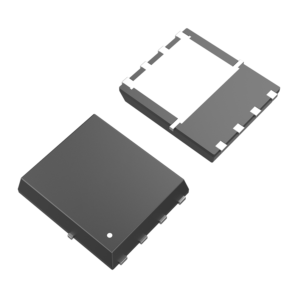
High-performance package Mosfets for power electronics applications
The leading manufacturer and supplier of power management and energy efficient semiconductor solutions, {} has recently introduced its latest Dpak-3 Package Mosfets to the market. This new product signifies a significant advancement in power management technology and is set to revolutionize the way power is handled in various applications.The Dpak-3 Package Mosfets are designed to provide high efficiency and reliability, making them ideal for use in a wide range of industrial and consumer electronics applications. The innovative design of these Mosfets allows for improved thermal performance and lower on-resistance, leading to reduced power loss and higher efficiency.With the increasing demand for more energy-efficient solutions, {} is committed to providing cutting-edge technologies that meet the needs of the modern world. The Dpak-3 Package Mosfets are a testament to this commitment, offering a combination of high performance and reliability that is unmatched in the industry.The Dpak-3 Package Mosfets are suitable for a variety of applications, including power supplies, motor control, LED lighting, and battery management systems. This versatility makes them an attractive option for designers and engineers looking to optimize power management in their products.One of the key features of the Dpak-3 Package Mosfets is their compact size, which allows for easy integration into existing designs without sacrificing performance. This makes them an ideal choice for applications where space is limited, such as portable electronics and automation equipment.In addition to their high performance, the Dpak-3 Package Mosfets also boast excellent reliability and ruggedness, making them suitable for use in harsh operating environments. This ensures that the devices can withstand extreme conditions without compromising their performance, making them an ideal choice for industrial applications.The introduction of the Dpak-3 Package Mosfets further solidifies {}'s position as a leader in the power management and energy efficient semiconductor market. With a strong focus on innovation and quality, the company continues to deliver solutions that address the evolving needs of the industry.The Dpak-3 Package Mosfets are just one example of {}'s commitment to pushing the boundaries of power management technology. As the demand for energy-efficient solutions continues to grow, the company remains dedicated to providing products that meet and exceed the expectations of its customers.In conclusion, the introduction of the Dpak-3 Package Mosfets represents a significant milestone for {}. With their high performance, reliability, and versatility, these Mosfets are set to make a lasting impact on the power management industry. As the company continues to innovate and develop new technologies, it is poised to remain at the forefront of the semiconductor market for years to come.
Ultimate Guide to Understanding Channel Enhancement MOSFET Technology
P Channel Enhancement Mosfet is a cutting-edge technology that is revolutionizing the semiconductor industry. This advanced power management component has been developed by a leading company in the field of electronics and semiconductors, {Company Name}.{Company Name} is a globally renowned corporation that specializes in designing and manufacturing high-performance semiconductor products. With a strong focus on research and development, innovation, and customer satisfaction, {Company Name} has earned a reputation for delivering top-quality products that cater to a wide range of applications in various industries.The P Channel Enhancement Mosfet, developed by {Company Name}, is a game-changer in the world of power management. It offers exceptional performance, efficiency, and reliability, making it an ideal choice for a wide range of applications, including automotive, industrial, consumer electronics, and telecommunications.One of the key features of the P Channel Enhancement Mosfet is its high power density, which allows for significant energy savings and improved system performance. This makes it an excellent choice for applications where power efficiency is critical, such as electric vehicles, solar inverters, and power supplies.In addition to its impressive power density, the P Channel Enhancement Mosfet also offers low on-resistance and high current-carrying capability, making it well-suited for high-power applications. Its advanced design and construction ensure minimal power loss and heat dissipation, leading to improved overall system efficiency.Moreover, the P Channel Enhancement Mosfet from {Company Name} boasts excellent thermal performance, ensuring reliable operation even in harsh environmental conditions. Its robust design and construction make it suitable for a wide range of operating temperatures, further enhancing its versatility and applicability in various industries.Furthermore, {Company Name} prides itself on its commitment to quality and reliability. The P Channel Enhancement Mosfet undergoes rigorous testing and quality control measures to ensure that it meets the highest industry standards. This ensures that customers can trust the performance and longevity of the product, providing peace of mind and confidence in their applications.The P Channel Enhancement Mosfet is just one example of the innovative solutions that {Company Name} continues to develop. With a strong focus on pushing the boundaries of semiconductor technology, {Company Name} is committed to driving industry advancements and delivering value to its customers.As a leader in the semiconductor industry, {Company Name} continues to invest in research and development, with a dedicated team of engineers and scientists working tirelessly to innovate and create cutting-edge solutions. The company's relentless pursuit of excellence and its passion for technology have positioned it as a trusted and respected partner for businesses across various sectors.In conclusion, the P Channel Enhancement Mosfet from {Company Name} is a testament to the company's commitment to delivering innovative, high-performance semiconductor solutions to the market. With its exceptional power density, efficiency, reliability, and versatility, this advanced power management component is set to make a significant impact across a wide range of industries, setting new benchmarks for performance and value. As {Company Name} continues to drive innovation and excellence, it is poised to lead the way in shaping the future of the semiconductor industry.
Understanding the Depletion Type N Channel Mosfet: A Comprehensive Guide
Depletion Type N Channel Mosfet Revolutionizes Power Management TechnologyIn today's fast-paced and technologically advanced world, the demand for efficient and reliable power management solutions has never been greater. With the increasing reliance on electronic devices in both consumer and industrial sectors, the need for power-efficient components has become a top priority for engineers and designers.Addressing this need, {Company Name}, a leading global provider of semiconductor solutions, has recently unveiled its latest breakthrough in power management technology - the Depletion Type N Channel Mosfet. This innovative component is set to revolutionize the way power is managed and controlled, offering a range of benefits and applications for a variety of industries.The Depletion Type N Channel Mosfet is a type of metal-oxide-semiconductor field-effect transistor (MOSFET) that operates on the principle of a depletion mode device. This means that it is normally-on without the application of a gate voltage, making it ideal for applications requiring a constant conductance.One of the key advantages of the Depletion Type N Channel Mosfet is its ability to operate at higher temperatures and voltages compared to traditional MOSFETs, making it a more reliable and robust solution for power management in demanding environments. This capability opens up a wide range of new applications for the component, including automotive, industrial, and aerospace systems where high-temperature operation is required.The Depletion Type N Channel Mosfet also offers improved power efficiency, with lower on-state resistance and higher current carrying capability compared to standard MOSFET devices. This means that it can handle higher power levels while minimizing power loss, making it an attractive solution for applications where energy efficiency is a top priority.In addition, the Depletion Type N Channel Mosfet features enhanced ruggedness and reliability, making it suitable for use in harsh operating conditions. Its ability to withstand electrical and thermal stress makes it an ideal choice for mission-critical systems where reliability is paramount.{Company Name} has a long-standing reputation for delivering high-quality semiconductor solutions to a diverse customer base. With a commitment to innovation and excellence, the company has continuously pushed the boundaries of technology to develop cutting-edge components that meet the evolving needs of the industry.The introduction of the Depletion Type N Channel Mosfet is a testament to {Company Name}'s dedication to providing advanced power management solutions that empower engineers and designers to create the next generation of electronic devices and systems. By combining state-of-the-art technology with a deep understanding of market demands, {Company Name} continues to set new benchmarks in the semiconductor industry.The unveiling of the Depletion Type N Channel Mosfet represents a significant milestone for {Company Name}, as it further solidifies the company's position as a leader in the semiconductor market. With its innovative features and unparalleled performance, the component is expected to gain widespread adoption across a range of industries, driving new possibilities for power management and control.As the demand for more efficient and reliable power management solutions continues to grow, {Company Name} remains at the forefront of innovation, consistently delivering game-changing technologies that shape the future of the industry. The Depletion Type N Channel Mosfet is a clear example of {Company Name}'s commitment to driving progress and creating value for its customers through advanced semiconductor solutions.
Advanced Dual-Gate Mosfet Technology Unveiled in Latest News
Today, we are excited to share with you the latest innovation from {Company Name}. The N channel dual gate MOSFET is set to revolutionize the semiconductor industry and pave the way for significant advancements in electronics and technology.The N channel dual gate MOSFET is a cutting-edge semiconductor device with two gates, allowing for enhanced control and performance. This innovative technology offers superior efficiency and functionality compared to traditional single gate MOSFETs, making it a game-changer in the world of electronics.With the rise of smart devices, electric vehicles, and renewable energy systems, the demand for high-performance, energy-efficient semiconductor devices is at an all-time high. The N channel dual gate MOSFET is poised to meet this demand and drive the next wave of technological advancements.At {Company Name}, we are committed to pushing the boundaries of innovation and delivering groundbreaking solutions to our customers. With the introduction of the N channel dual gate MOSFET, we are proud to be at the forefront of the semiconductor industry, driving progress and shaping the future of technology.Our team of dedicated engineers and researchers has worked tirelessly to develop and perfect the N channel dual gate MOSFET, ensuring that it meets the highest standards of quality and performance. Through rigorous testing and optimization, we have created a semiconductor device that offers unparalleled efficiency, reliability, and versatility.The N channel dual gate MOSFET is designed to be a versatile and efficient solution for a wide range of applications, including power supplies, motor control, RF amplifiers, and more. Its advanced design and superior performance make it an ideal choice for use in cutting-edge technologies and emerging industries.One of the key advantages of the N channel dual gate MOSFET is its ability to deliver high power density while maintaining low on-resistance, resulting in improved efficiency and reduced power loss. This is particularly important in the context of electric vehicles and renewable energy systems, where maximizing energy efficiency is a top priority.In addition to its impressive performance, the N channel dual gate MOSFET also offers enhanced control capabilities, thanks to its dual gate design. This allows for greater flexibility and precision in managing the flow of current, making it an ideal choice for applications that require precise power management and control.The introduction of the N channel dual gate MOSFET underscores {Company Name}'s commitment to innovation and leadership in the semiconductor industry. We are proud to be at the forefront of developing technologies that have the potential to transform the way we live, work, and communicate.As we look to the future, we are excited about the possibilities that the N channel dual gate MOSFET presents. We believe that this groundbreaking semiconductor device will play a crucial role in shaping the next generation of electronics and technology, and we are thrilled to be leading the charge.In conclusion, the N channel dual gate MOSFET represents a major milestone in the semiconductor industry, offering superior performance, efficiency, and control capabilities. At {Company Name}, we are proud to be driving progress and shaping the future of technology through our commitment to innovation and excellence. We are confident that the N channel dual gate MOSFET will be a game-changer in the world of electronics, and we are excited to see the transformative impact it will have on the industry.
High-Performance 40A N-Channel Mosfet for Power Applications
N Channel Mosfet 40a: The Future of Power ManagementIn recent years, the demand for more efficient and reliable power management solutions has been on the rise. As industries continue to evolve and demand for energy-efficient products increases, it is essential for companies to stay ahead of the curve by developing products that can meet the needs of today's market. One company at the forefront of this innovation is {Company Name}.{Company Name} has been a leader in the development and manufacturing of electronic components for over a decade. With a strong focus on research and development, the company has continuously pushed the boundaries of power management technology to provide its customers with cutting-edge solutions. Their latest product, the N Channel Mosfet 40a, is a testament to their commitment to innovation and excellence.The N Channel Mosfet 40a is a high-performance power management solution that offers unparalleled efficiency and reliability. Designed to meet the needs of a wide range of industries, including automotive, industrial, and consumer electronics, this Mosfet has the potential to revolutionize power management. With a maximum amperage of 40a, it is capable of handling even the most demanding power requirements, making it an ideal choice for a wide range of applications.One of the key features of the N Channel Mosfet 40a is its low on-resistance, which minimizes power loss and maximizes efficiency. This, combined with its high switching speed, makes it the perfect choice for applications that require precise and responsive power management. Its compact size and lightweight design also make it easy to integrate into existing systems, making it a versatile solution for a wide range of applications.In addition to its technical capabilities, the N Channel Mosfet 40a is also designed with the end user in mind. Its robust construction and high durability ensure long-term reliability, while its easy installation and user-friendly interface make it accessible to a wide range of users. Furthermore, {Company Name} offers comprehensive technical support and after-sales service, ensuring that their customers can maximize the potential of this groundbreaking product.The launch of the N Channel Mosfet 40a represents a significant milestone for {Company Name} and is a testament to their dedication to providing innovative solutions to their customers. With this new product, they are well-positioned to meet the growing demand for energy-efficient power management solutions and to continue their legacy of excellence in the electronic components industry.Given the increasing demand for more efficient and reliable power management solutions, the N Channel Mosfet 40a has the potential to make a significant impact on the market. Its high performance, reliability, and versatility make it an ideal choice for a wide range of applications, and it is sure to be a popular choice among industry professionals.The N Channel Mosfet 40a is the latest innovation from {Company Name}, a company that has built a reputation for excellence in the electronic components industry. With their strong focus on research and development, as well as their commitment to providing high-quality products and exceptional customer support, they are well-positioned to continue leading the way in power management technology.As industries continue to evolve and demand for energy-efficient products increases, it is essential for companies to stay ahead of the curve by developing products that can meet the needs of today's market. With the launch of the N Channel Mosfet 40a, {Company Name} has demonstrated their commitment to innovation and excellence, and they are well-positioned to make a significant impact on the power management industry.
How P-Channel BJTs Are Used in Electrical Engineering
P Channel BJT Technology: Revolutionizing the Semiconductor IndustryIn today's ever-evolving technological landscape, the semiconductor industry plays a crucial role in powering the electronic devices that have become a ubiquitous part of our daily lives. One company that has been at the forefront of driving innovation in the semiconductor space is {}.{} is a leading provider of semiconductor solutions, with a strong focus on research and development. The company has been dedicated to producing cutting-edge technologies that are shaping the future of the semiconductor industry. One of the key innovations that {} has recently introduced is the P Channel BJT (Bipolar Junction Transistor) technology.P Channel BJT is a type of transistor that has garnered significant attention within the semiconductor industry due to its potential to revolutionize the way electronic devices are designed and manufactured. Unlike traditional NPN (Negative-Positive-Negative) transistors, P Channel BJT technology offers a range of benefits that make it an attractive choice for a wide variety of applications.P Channel BJT transistors offer improved efficiency, lower power consumption, and higher switching speeds, making them ideal for use in a range of electronic devices, from smartphones and tablets to high-performance computing systems. The technology also boasts enhanced thermal performance, allowing for better heat dissipation in electronic devices, which is crucial for maintaining their reliability and longevity.One of the most significant advantages of P Channel BJT technology is its compatibility with existing semiconductor manufacturing processes. This means that companies in the semiconductor industry can seamlessly integrate P Channel BJT transistors into their production lines, without the need for major retooling or overhauls. This compatibility makes it easier for semiconductor manufacturers to adopt P Channel BJT technology, facilitating a smoother transition towards more efficient and high-performance electronic devices.{} has been at the forefront of developing and commercializing P Channel BJT technology, leveraging its expertise in semiconductor design and manufacturing. The company's commitment to innovation and engineering excellence has allowed it to push the boundaries of what is possible in the semiconductor industry, paving the way for new possibilities and opportunities for electronic devices.The introduction of P Channel BJT technology by {} has sparked renewed interest in the semiconductor industry, with many industry experts lauding its potential to drive significant advancements in electronic device design and performance. As the demand for electronic devices continues to rise, the need for more efficient and reliable semiconductor solutions becomes increasingly critical, and P Channel BJT technology is well-positioned to meet these growing demands.With the continued development and refinement of P Channel BJT technology, {} is poised to solidify its position as a leader in the semiconductor industry. The company's dedication to innovation and its track record of delivering high-quality semiconductor solutions have positioned it as a key player in driving the future of electronic devices.In conclusion, the introduction of P Channel BJT technology by {} represents a significant milestone in the semiconductor industry. With its potential to revolutionize electronic device design and manufacturing, P Channel BJT technology is set to play a pivotal role in shaping the future of the semiconductor industry. As {} continues to push the boundaries of innovation, the impact of P Channel BJT technology is expected to be felt across a wide range of electronic devices, driving new possibilities and opportunities for the industry as a whole.
High Voltage Mosfet with 2A Current Capacity
N Channel Mosfet 30v 2a (need remove brand name) has recently been making waves in the electronics industry, providing an innovative and efficient solution for power management and control. This revolutionary technology has been developed by a leading company in the field of semiconductor components, known for its commitment to quality and reliability.With the increasing demand for high-performance power management solutions, the N Channel Mosfet 30v 2a (need remove brand name) has emerged as a game-changer in the market. Its unique design and advanced features make it an ideal choice for a wide range of applications, from consumer electronics to industrial automation.One of the key advantages of the N Channel Mosfet 30v 2a (need remove brand name) is its high power efficiency, which allows for better energy management and reduced power consumption. This is particularly important in today's energy-conscious world, where reducing power usage and increasing efficiency are critical goals for businesses and consumers alike.Furthermore, the N Channel Mosfet 30v 2a (need remove brand name) is also known for its robust construction and high reliability, making it suitable for even the most demanding operating conditions. This is a testament to the company's dedication to delivering products that meet the highest standards of performance and durability.In addition, the N Channel Mosfet 30v 2a (need remove brand name) is designed for ease of use and integration, with a range of features that make it simple to implement into a variety of designs and applications. This versatility makes it an attractive option for designers and engineers looking for a flexible and adaptable power management solution.The company behind the N Channel Mosfet 30v 2a (need remove brand name) is known for its strong commitment to research and development, constantly pushing the boundaries of semiconductor technology to deliver products that exceed customer expectations. Its team of experts and engineers are dedicated to staying ahead of the curve, ensuring that their products remain at the forefront of innovation and performance.Moreover, the company's dedication to quality and reliability is reflected in its stringent testing and quality control processes, which ensure that every product that leaves its facilities meets the highest standards of excellence. This commitment to quality has earned the company a reputation for being a trusted and reliable partner for businesses around the world.The N Channel Mosfet 30v 2a (need remove brand name) is just one example of the company's ongoing commitment to innovation and excellence. With a strong focus on customer satisfaction and a drive to continuously improve, the company is poised to remain a leader in the field of semiconductor components for years to come.In conclusion, the N Channel Mosfet 30v 2a (need remove brand name) is a groundbreaking technology that is set to revolutionize the power management industry. With its high efficiency, reliability, and ease of use, it is a versatile solution that is well-suited to a wide range of applications. Coupled with the company's dedication to quality and innovation, the N Channel Mosfet 30v 2a (need remove brand name) is undoubtedly a force to be reckoned with in the world of semiconductor components.
High performance 30v 75a N Channel Mosfet for efficient power management
(N Channel Mosfet 30v 75a) is a new high-performance power MOSFET designed for a wide range of applications in the electronics industry. This innovative new product is making waves in the industry due to its superior performance and reliability, setting a new standard for power MOSFET technology.The (N Channel MOSFET 30v 75a) is designed to meet the demands of modern electronics, offering a high drain current of 75A and a low on-resistance. This means that it can handle high power and voltage levels, making it ideal for use in power supply units, motor control, and other high-power applications. The (N Channel Mosfet 30v 75a) also features a low gate charge and a fast switching speed, allowing for efficient and precise control of power flow.The (N Channel Mosfet 30v 75a) is built with the latest semiconductor technology, ensuring that it delivers optimal performance and reliability. It is also designed to operate in harsh environments, with a wide temperature range and excellent thermal performance. This makes it suitable for use in a variety of industrial and automotive applications, where reliability and ruggedness are essential.In addition to its technical specifications, the (N Channel Mosfet 30v 75a) also boasts a compact and lightweight design, making it easy to integrate into a wide range of electronic devices and systems. Its small form factor and high power handling capability make it an ideal choice for applications where space is at a premium, such as in portable electronics and handheld devices.The (N Channel Mosfet 30v 75a) is the latest addition to {}'s extensive lineup of power MOSFETs, which are known for their high performance and quality. As a leading manufacturer of semiconductors, {} has a long history of delivering innovative solutions to the electronics industry, and the (N Channel Mosfet 30v 75a) is no exception.{} is dedicated to pushing the boundaries of power MOSFET technology, and the (N Channel Mosfet 30v 75a) is a testament to that commitment. With its high performance, reliability, and versatility, this new product is set to become the go-to choice for engineers and designers looking for a high-power MOSFET solution.In conclusion, the (N Channel Mosfet 30v 75a) is a game-changing new product from {}, offering unmatched performance, reliability, and versatility. With its high power handling capability, fast switching speed, and rugged design, it is poised to become a staple in a wide range of electronic applications, setting a new standard for power MOSFET technology. As {} continues to drive innovation in the semiconductor industry, the (N Channel Mosfet 30v 75a) is a clear example of their commitment to delivering cutting-edge solutions to meet the evolving needs of the electronics market.
How to effectively utilize a P Channel BJT for improved performance
P Channel BJT, A Revolutionary Breakthrough in Semiconductor Technology[Company Name] is thrilled to introduce its latest innovation in semiconductor technology with the launch of P Channel BJT, a groundbreaking development that is set to revolutionize the industry. With its superior performance and unique features, this new product is poised to create waves in the market and set a new benchmark for excellence in semiconductor devices.P Channel BJT is a high-performance, power efficient semiconductor device that has been meticulously designed and engineered to deliver exceptional performance and reliability. Equipped with advanced technology and cutting-edge materials, this new product offers a range of benefits that set it apart from traditional BJTs and other semiconductor devices.One of the key advantages of P Channel BJT is its superior power efficiency, which is achieved through its innovative design and optimized performance characteristics. This allows for lower power consumption and higher energy efficiency, making it an ideal choice for applications that require high performance and reliability, while also prioritizing energy savings and environmental sustainability.In addition to its power efficiency, P Channel BJT also offers superior thermal management, enabling it to operate at higher temperatures and in harsh environments without compromising its performance. This makes it an ideal solution for a wide range of demanding applications, including automotive, industrial, and consumer electronics, where reliability and durability are essential.Furthermore, P Channel BJT boasts an enhanced switching speed and performance, allowing for faster and more efficient operation in high-speed applications. This makes it an ideal choice for applications that require rapid response times and precision control, such as power management systems, motor control, and high-frequency amplifiers.With its exceptional performance and advanced features, P Channel BJT is set to redefine the standards for semiconductor devices and open up new possibilities for innovation and advancement in various industries. Its unique combination of power efficiency, thermal management, and high-speed performance makes it a game-changing solution for engineers and designers, offering them a versatile and reliable platform to develop next-generation products and systems.The launch of P Channel BJT marks a significant milestone for [Company Name], showcasing its commitment to pushing the boundaries of semiconductor technology and delivering innovative solutions that address the evolving needs of the industry. Leveraging its expertise in semiconductor design and manufacturing, the company has developed P Channel BJT as a result of extensive research and development, ensuring that it meets the highest standards of quality and performance.As part of its commitment to excellence, [Company Name] has invested heavily in state-of-the-art facilities and cutting-edge manufacturing processes to ensure the production of P Channel BJT adheres to the highest quality and performance standards. This dedication to quality and innovation underscores the company's position as a leader in the semiconductor industry, and its ability to deliver groundbreaking solutions to its customers.Looking ahead, P Channel BJT is poised to make a lasting impact in the semiconductor market, setting a new precedent for power efficiency, thermal management, and high-speed performance. Its arrival is expected to create new opportunities for innovation and growth, driving the development of advanced products and systems that leverage its unique capabilities and benefits.In conclusion, the launch of P Channel BJT represents a significant advancement in semiconductor technology, offering a game-changing solution that sets new standards for performance and reliability. With its exceptional power efficiency, thermal management, and high-speed performance, this revolutionary product has the potential to unlock new possibilities and drive innovation across various industries, cementing its position as a pioneering development in the world of semiconductors.
Learn About To252aa Dpak Mosfet and Its Uses in Electronic Devices
Today, [Company Name] is proud to announce the release of our latest technological innovation, the TO252AA DPAK MOSFET. As a leading global supplier of semiconductor components, we continue to strive for excellence in providing cutting-edge solutions for the electronics industry.The TO252AA DPAK MOSFET is a high-performance, low on-resistance device that is designed to meet the demands of a wide range of applications, including power supplies, motor control, and lighting. With its compact size and efficient power handling capabilities, this MOSFET is poised to revolutionize the way electronic devices are designed and operated.This new product is a testament to our commitment to research and development. Our team of experienced engineers and researchers have worked tirelessly to create a MOSFET that not only meets the current industry standards, but also exceeds them. By leveraging the latest technologies and manufacturing techniques, we have been able to produce a MOSFET that offers unparalleled performance and reliability.In addition to its technical capabilities, the TO252AA DPAK MOSFET also reflects our dedication to sustainability. By utilizing advanced materials and production processes, we have been able to minimize the environmental impact of this product, making it an eco-friendly choice for our customers.Furthermore, our extensive quality control measures ensure that every MOSFET that leaves our facilities meets the highest standards of performance and durability. This commitment to quality is a hallmark of our company, and is evident in every product we deliver to our customers.The release of the TO252AA DPAK MOSFET represents a significant milestone for [Company Name]. With this new addition to our product lineup, we are well-positioned to further solidify our position as a leader in the semiconductor industry. We are confident that this MOSFET will not only meet the current needs of our customers, but also pave the way for future advancements in electronic technology.In conclusion, the introduction of the TO252AA DPAK MOSFET is a testament to the innovative spirit and technical expertise that defines [Company Name]. We are proud to continue our tradition of excellence and look forward to the positive impact that this new product will have on the electronics industry. As we move forward, we remain committed to pushing the boundaries of what is possible in semiconductor technology, and are excited to see the ways in which the TO252AA DPAK MOSFET will shape the future of electronic devices.
High-performance package Mosfets for power electronics applications
The leading manufacturer and supplier of power management and energy efficient semiconductor solutions, {} has recently introduced its latest Dpak-3 Package Mosfets to the market. This new product signifies a significant advancement in power management technology and is set to revolutionize the way power is handled in various applications.The Dpak-3 Package Mosfets are designed to provide high efficiency and reliability, making them ideal for use in a wide range of industrial and consumer electronics applications. The innovative design of these Mosfets allows for improved thermal performance and lower on-resistance, leading to reduced power loss and higher efficiency.With the increasing demand for more energy-efficient solutions, {} is committed to providing cutting-edge technologies that meet the needs of the modern world. The Dpak-3 Package Mosfets are a testament to this commitment, offering a combination of high performance and reliability that is unmatched in the industry.The Dpak-3 Package Mosfets are suitable for a variety of applications, including power supplies, motor control, LED lighting, and battery management systems. This versatility makes them an attractive option for designers and engineers looking to optimize power management in their products.One of the key features of the Dpak-3 Package Mosfets is their compact size, which allows for easy integration into existing designs without sacrificing performance. This makes them an ideal choice for applications where space is limited, such as portable electronics and automation equipment.In addition to their high performance, the Dpak-3 Package Mosfets also boast excellent reliability and ruggedness, making them suitable for use in harsh operating environments. This ensures that the devices can withstand extreme conditions without compromising their performance, making them an ideal choice for industrial applications.The introduction of the Dpak-3 Package Mosfets further solidifies {}'s position as a leader in the power management and energy efficient semiconductor market. With a strong focus on innovation and quality, the company continues to deliver solutions that address the evolving needs of the industry.The Dpak-3 Package Mosfets are just one example of {}'s commitment to pushing the boundaries of power management technology. As the demand for energy-efficient solutions continues to grow, the company remains dedicated to providing products that meet and exceed the expectations of its customers.In conclusion, the introduction of the Dpak-3 Package Mosfets represents a significant milestone for {}. With their high performance, reliability, and versatility, these Mosfets are set to make a lasting impact on the power management industry. As the company continues to innovate and develop new technologies, it is poised to remain at the forefront of the semiconductor market for years to come.
Ultimate Guide to Understanding Channel Enhancement MOSFET Technology
P Channel Enhancement Mosfet is a cutting-edge technology that is revolutionizing the semiconductor industry. This advanced power management component has been developed by a leading company in the field of electronics and semiconductors, {Company Name}.{Company Name} is a globally renowned corporation that specializes in designing and manufacturing high-performance semiconductor products. With a strong focus on research and development, innovation, and customer satisfaction, {Company Name} has earned a reputation for delivering top-quality products that cater to a wide range of applications in various industries.The P Channel Enhancement Mosfet, developed by {Company Name}, is a game-changer in the world of power management. It offers exceptional performance, efficiency, and reliability, making it an ideal choice for a wide range of applications, including automotive, industrial, consumer electronics, and telecommunications.One of the key features of the P Channel Enhancement Mosfet is its high power density, which allows for significant energy savings and improved system performance. This makes it an excellent choice for applications where power efficiency is critical, such as electric vehicles, solar inverters, and power supplies.In addition to its impressive power density, the P Channel Enhancement Mosfet also offers low on-resistance and high current-carrying capability, making it well-suited for high-power applications. Its advanced design and construction ensure minimal power loss and heat dissipation, leading to improved overall system efficiency.Moreover, the P Channel Enhancement Mosfet from {Company Name} boasts excellent thermal performance, ensuring reliable operation even in harsh environmental conditions. Its robust design and construction make it suitable for a wide range of operating temperatures, further enhancing its versatility and applicability in various industries.Furthermore, {Company Name} prides itself on its commitment to quality and reliability. The P Channel Enhancement Mosfet undergoes rigorous testing and quality control measures to ensure that it meets the highest industry standards. This ensures that customers can trust the performance and longevity of the product, providing peace of mind and confidence in their applications.The P Channel Enhancement Mosfet is just one example of the innovative solutions that {Company Name} continues to develop. With a strong focus on pushing the boundaries of semiconductor technology, {Company Name} is committed to driving industry advancements and delivering value to its customers.As a leader in the semiconductor industry, {Company Name} continues to invest in research and development, with a dedicated team of engineers and scientists working tirelessly to innovate and create cutting-edge solutions. The company's relentless pursuit of excellence and its passion for technology have positioned it as a trusted and respected partner for businesses across various sectors.In conclusion, the P Channel Enhancement Mosfet from {Company Name} is a testament to the company's commitment to delivering innovative, high-performance semiconductor solutions to the market. With its exceptional power density, efficiency, reliability, and versatility, this advanced power management component is set to make a significant impact across a wide range of industries, setting new benchmarks for performance and value. As {Company Name} continues to drive innovation and excellence, it is poised to lead the way in shaping the future of the semiconductor industry.
Understanding the Depletion Type N Channel Mosfet: A Comprehensive Guide
Depletion Type N Channel Mosfet Revolutionizes Power Management TechnologyIn today's fast-paced and technologically advanced world, the demand for efficient and reliable power management solutions has never been greater. With the increasing reliance on electronic devices in both consumer and industrial sectors, the need for power-efficient components has become a top priority for engineers and designers.Addressing this need, {Company Name}, a leading global provider of semiconductor solutions, has recently unveiled its latest breakthrough in power management technology - the Depletion Type N Channel Mosfet. This innovative component is set to revolutionize the way power is managed and controlled, offering a range of benefits and applications for a variety of industries.The Depletion Type N Channel Mosfet is a type of metal-oxide-semiconductor field-effect transistor (MOSFET) that operates on the principle of a depletion mode device. This means that it is normally-on without the application of a gate voltage, making it ideal for applications requiring a constant conductance.One of the key advantages of the Depletion Type N Channel Mosfet is its ability to operate at higher temperatures and voltages compared to traditional MOSFETs, making it a more reliable and robust solution for power management in demanding environments. This capability opens up a wide range of new applications for the component, including automotive, industrial, and aerospace systems where high-temperature operation is required.The Depletion Type N Channel Mosfet also offers improved power efficiency, with lower on-state resistance and higher current carrying capability compared to standard MOSFET devices. This means that it can handle higher power levels while minimizing power loss, making it an attractive solution for applications where energy efficiency is a top priority.In addition, the Depletion Type N Channel Mosfet features enhanced ruggedness and reliability, making it suitable for use in harsh operating conditions. Its ability to withstand electrical and thermal stress makes it an ideal choice for mission-critical systems where reliability is paramount.{Company Name} has a long-standing reputation for delivering high-quality semiconductor solutions to a diverse customer base. With a commitment to innovation and excellence, the company has continuously pushed the boundaries of technology to develop cutting-edge components that meet the evolving needs of the industry.The introduction of the Depletion Type N Channel Mosfet is a testament to {Company Name}'s dedication to providing advanced power management solutions that empower engineers and designers to create the next generation of electronic devices and systems. By combining state-of-the-art technology with a deep understanding of market demands, {Company Name} continues to set new benchmarks in the semiconductor industry.The unveiling of the Depletion Type N Channel Mosfet represents a significant milestone for {Company Name}, as it further solidifies the company's position as a leader in the semiconductor market. With its innovative features and unparalleled performance, the component is expected to gain widespread adoption across a range of industries, driving new possibilities for power management and control.As the demand for more efficient and reliable power management solutions continues to grow, {Company Name} remains at the forefront of innovation, consistently delivering game-changing technologies that shape the future of the industry. The Depletion Type N Channel Mosfet is a clear example of {Company Name}'s commitment to driving progress and creating value for its customers through advanced semiconductor solutions.
Advanced Dual-Gate Mosfet Technology Unveiled in Latest News
Today, we are excited to share with you the latest innovation from {Company Name}. The N channel dual gate MOSFET is set to revolutionize the semiconductor industry and pave the way for significant advancements in electronics and technology.The N channel dual gate MOSFET is a cutting-edge semiconductor device with two gates, allowing for enhanced control and performance. This innovative technology offers superior efficiency and functionality compared to traditional single gate MOSFETs, making it a game-changer in the world of electronics.With the rise of smart devices, electric vehicles, and renewable energy systems, the demand for high-performance, energy-efficient semiconductor devices is at an all-time high. The N channel dual gate MOSFET is poised to meet this demand and drive the next wave of technological advancements.At {Company Name}, we are committed to pushing the boundaries of innovation and delivering groundbreaking solutions to our customers. With the introduction of the N channel dual gate MOSFET, we are proud to be at the forefront of the semiconductor industry, driving progress and shaping the future of technology.Our team of dedicated engineers and researchers has worked tirelessly to develop and perfect the N channel dual gate MOSFET, ensuring that it meets the highest standards of quality and performance. Through rigorous testing and optimization, we have created a semiconductor device that offers unparalleled efficiency, reliability, and versatility.The N channel dual gate MOSFET is designed to be a versatile and efficient solution for a wide range of applications, including power supplies, motor control, RF amplifiers, and more. Its advanced design and superior performance make it an ideal choice for use in cutting-edge technologies and emerging industries.One of the key advantages of the N channel dual gate MOSFET is its ability to deliver high power density while maintaining low on-resistance, resulting in improved efficiency and reduced power loss. This is particularly important in the context of electric vehicles and renewable energy systems, where maximizing energy efficiency is a top priority.In addition to its impressive performance, the N channel dual gate MOSFET also offers enhanced control capabilities, thanks to its dual gate design. This allows for greater flexibility and precision in managing the flow of current, making it an ideal choice for applications that require precise power management and control.The introduction of the N channel dual gate MOSFET underscores {Company Name}'s commitment to innovation and leadership in the semiconductor industry. We are proud to be at the forefront of developing technologies that have the potential to transform the way we live, work, and communicate.As we look to the future, we are excited about the possibilities that the N channel dual gate MOSFET presents. We believe that this groundbreaking semiconductor device will play a crucial role in shaping the next generation of electronics and technology, and we are thrilled to be leading the charge.In conclusion, the N channel dual gate MOSFET represents a major milestone in the semiconductor industry, offering superior performance, efficiency, and control capabilities. At {Company Name}, we are proud to be driving progress and shaping the future of technology through our commitment to innovation and excellence. We are confident that the N channel dual gate MOSFET will be a game-changer in the world of electronics, and we are excited to see the transformative impact it will have on the industry.