
High-performance 80v N-channel Mosfet for efficient power management
By:Admin
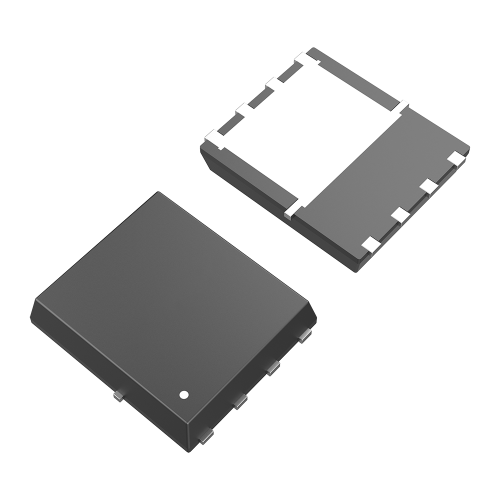
The 80V N-Channel MOSFET is the latest addition to {}'s extensive portfolio of high-performance semiconductor solutions. With its advanced design and state-of-the-art manufacturing process, this new MOSFET promises to deliver superior performance and reliability in a variety of demanding applications. By leveraging the latest advancements in semiconductor technology, {} has once again demonstrated its commitment to innovation and excellence in the field of power electronics.
One of the key features of the 80V N-Channel MOSFET is its high voltage capability, which allows it to efficiently handle higher power levels than traditional MOSFETs. This makes it an ideal choice for applications that require high power density and energy efficiency, such as electric vehicles, industrial motor drives, and power supplies. Additionally, the device's low on-resistance and low gate charge enable it to minimize power losses and improve overall system efficiency, making it an attractive option for designers and engineers looking to optimize the performance of their systems.
In addition to its impressive electrical performance, the 80V N-Channel MOSFET also offers a number of features that make it easy to use and integrate into existing designs. Its compact and lightweight package, for example, makes it suitable for space-constrained applications, while its robust and reliable construction ensures long-term performance in harsh operating environments. Furthermore, {}'s commitment to quality and reliability means that customers can trust the 80V N-Channel MOSFET to deliver consistent and dependable performance over its operational lifetime.
The introduction of the 80V N-Channel MOSFET represents a significant milestone for {} and reinforces the company's position as a leading provider of high-performance semiconductor solutions. With its unparalleled combination of performance, efficiency, and reliability, this new MOSFET is poised to set new standards for power electronics and enable the development of innovative and energy-efficient systems across a wide range of industries.
"We are excited to introduce the 80V N-Channel MOSFET to the market," said [spokesperson] of {}. "This new product represents the culmination of our extensive research and development efforts, and we believe it will make a significant impact on the industry. With its advanced performance and features, the 80V N-Channel MOSFET is well-positioned to address the evolving needs of our customers and enable the development of next-generation power electronic systems."
The 80V N-Channel MOSFET is now available for sampling, and volume production is expected to begin in the coming months. With its groundbreaking performance and advanced features, this new MOSFET is set to become an essential building block for the development of high-performance and energy-efficient electronic systems. As the demand for more powerful and efficient electronic devices continues to grow, the 80V N-Channel MOSFET is poised to play a crucial role in shaping the future of power electronics and enabling the development of innovative and sustainable technologies.
Company News & Blog
- Affordable Microcontroller Options for Your Project
We are pleased to introduce our latest innovation in the field of microcontrollers – a low-cost, high-performance solution that is set to revolutionize the industry. Our new microcontroller, which we are calling the A1 Microcontroller, offers a perfect balance of performance, power efficiency, and affordability, making it an ideal choice for a wide range of applications.The A1 Microcontroller features a powerful ARM Cortex-M4 processor, which provides high-speed processing capabilities and supports a wide variety of peripherals and interfaces. This makes it suitable for a wide range of applications, including Internet of Things (IoT) devices, smart home appliances, industrial automation, and consumer electronics.One of the key features of the A1 Microcontroller is its low power consumption, which makes it an ideal choice for battery-powered devices. This, combined with its small form factor and low cost, makes it a perfect fit for applications where power efficiency and cost-effectiveness are crucial.In addition to its hardware capabilities, the A1 Microcontroller is supported by a comprehensive software development ecosystem, which includes a robust Integrated Development Environment (IDE) and a wide range of software libraries and tools. This makes it easy for developers to get started with the A1 Microcontroller and quickly build and deploy their applications.The A1 Microcontroller is also backed by our company's commitment to quality and reliability. We have a strong track record of delivering high-quality products and providing excellent customer support, and we are confident that the A1 Microcontroller will live up to our customers' expectations.Our goal with the A1 Microcontroller is to provide a high-performance, low-cost solution that empowers developers and innovators to bring their ideas to life. We believe that the A1 Microcontroller has the potential to drive innovation and create new opportunities in the embedded systems industry.We are excited to bring the A1 Microcontroller to the market, and we are confident that it will be a game-changer for developers and engineers around the world. With its powerful hardware, low power consumption, and affordable price point, we believe that the A1 Microcontroller will open up a world of possibilities for the next generation of embedded systems.To learn more about the A1 Microcontroller and how it can benefit your next project, please visit our website or contact our sales team. We are looking forward to working with you to unleash the full potential of the A1 Microcontroller and help you bring your ideas to life. Thank you for your continued support, and we look forward to the exciting journey ahead with the A1 Microcontroller.
Highly Efficient To-252-3 Dpak Mosfet: Everything You Need to Know
The To-252-3 Dpak Mosfet, a new and innovative semiconductor device, is set to revolutionize the electronics industry. This powerful, efficient, and versatile component is manufactured by a leading company in the field of semiconductor technology. With its advanced design and superior performance, the To-252-3 Dpak Mosfet is poised to become an essential part of modern electronic devices and systems.The To-252-3 Dpak Mosfet is a type of metal-oxide-semiconductor field-effect transistor (MOSFET) that is designed to handle high power and high frequency applications. It is built using cutting-edge technology and state-of-the-art manufacturing processes, resulting in exceptional performance and reliability. The To-252-3 Dpak Mosfet is capable of delivering high power density, low on-state resistance, and fast switching speeds, making it an ideal choice for a wide range of electronic applications.The company behind the To-252-3 Dpak Mosfet is a global leader in the development and production of semiconductor devices. With a strong focus on innovation and quality, the company has established itself as a trusted partner for customers in various industries, including automotive, industrial, consumer electronics, and telecommunications. The company's commitment to excellence and customer satisfaction has helped it build a solid reputation in the semiconductor industry.The To-252-3 Dpak Mosfet is designed to meet the growing demand for high-performance and energy-efficient semiconductor solutions. Its compact size and high power density make it suitable for use in compact electronic devices, such as smartphones, tablets, and wearable technology. In addition, its robust design and high reliability make it an ideal choice for demanding industrial and automotive applications.One of the key features of the To-252-3 Dpak Mosfet is its low on-state resistance, which allows for efficient power conversion and minimizes energy loss. This makes it an ideal choice for power management and control applications, where energy efficiency and reliability are crucial. With the To-252-3 Dpak Mosfet, designers and engineers can create more efficient and reliable electronic systems, enabling new possibilities in various industries.The To-252-3 Dpak Mosfet is also designed for fast switching speeds, allowing for superior performance in high frequency applications. This feature is particularly important in telecommunications, data communication, and power supply systems, where fast and efficient switching is essential. With its fast switching speeds, the To-252-3 Dpak Mosfet enables the development of advanced electronic systems that can meet the growing demands of modern technology.In conclusion, the To-252-3 Dpak Mosfet represents a significant advancement in semiconductor technology. Its high power density, low on-state resistance, and fast switching speeds make it an ideal choice for a wide range of electronic applications. With the backing of a leading semiconductor company, the To-252-3 Dpak Mosfet is set to make a significant impact on the electronics industry, enabling the development of more efficient, reliable, and innovative electronic systems. As electronic devices continue to advance in sophistication, the To-252-3 Dpak Mosfet will play a crucial role in shaping the future of technology.
New N-Channel Enhancement Technology: What You Need to Know
N-Channel enhancement technology is a groundbreaking innovation in the field of semiconductor devices that has the potential to revolutionize electronic devices. This technology has been developed by a leading semiconductor company, {Company}, which is known for its cutting-edge research and development in the electronics industry.With the rapid advancement in technology, the demand for better and more efficient electronic devices has been growing exponentially. The introduction of N-Channel enhancement technology is a significant development that has the potential to address this demand by making electronic devices more efficient and powerful.N-Channel enhancement technology is based on the principle of using a special type of semiconductor material to enhance the performance of electronic devices. This technology allows for better control of the flow of charge carriers, which results in improved power efficiency and faster switching speed. As a result, electronic devices that are equipped with N-Channel enhancement technology can operate more efficiently and deliver better performance than traditional devices.One of the key advantages of N-Channel enhancement technology is its ability to reduce power consumption. By improving the efficiency of charge carrier flow, this technology can significantly reduce the amount of power that electronic devices consume, leading to longer battery life and lower energy costs. This is particularly important in today's world, where energy conservation is a critical concern.In addition to power efficiency, N-Channel enhancement technology also offers faster switching speeds, which can lead to better overall performance of electronic devices. This means that devices equipped with this technology can process information more quickly, leading to improved responsiveness and better user experience.The potential applications of N-Channel enhancement technology are vast, ranging from smartphones and tablets to industrial equipment and power systems. By incorporating this technology into their products, manufacturers can create electronic devices that are not only more powerful and efficient, but also more environmentally friendly.{Company} has been at the forefront of developing N-Channel enhancement technology and has already integrated it into a range of semiconductor devices. The company's expertise in semiconductor design and manufacturing has enabled it to create cutting-edge products that leverage the benefits of this technology.With the introduction of N-Channel enhancement technology, {Company} has once again demonstrated its commitment to innovation and excellence in the semiconductor industry. The company's dedication to research and development has positioned it as a leader in the field, and its latest innovation is expected to have a significant impact on the electronic devices market.As the demand for more efficient and powerful electronic devices continues to grow, the introduction of N-Channel enhancement technology by {Company} is poised to be a game-changer. This technology has the potential to reshape the electronic devices market and provide consumers with better, more efficient products.In conclusion, N-Channel enhancement technology is a groundbreaking innovation that has the potential to revolutionize electronic devices. With its ability to improve power efficiency and switching speed, this technology is poised to redefine the capabilities of electronic devices. {Company}'s expertise in semiconductor design and manufacturing positions it as a key player in this field, and its introduction of N-Channel enhancement technology is expected to have a significant impact on the industry. As the demand for more efficient and powerful electronic devices continues to grow, the integration of this technology into products is likely to shape the future of the electronics market.
Advanced N-FETs: The Latest Breakthrough in Semiconductor Technology
N-FETs Revolutionize the Electronics Industry In recent years, technological advancements have revolutionized the electronics industry, and one of the key players driving this innovation is the introduction of N-FETs. These N-type Field-Effect Transistors have quickly gained prominence for their ability to significantly enhance electronic devices' performance and efficiency. With their ever-growing importance, the demand for N-FETs has skyrocketed, leading to a surge in production and sales.One of the companies at the forefront of this technological revolution is {}. Established in 2005, {} has been a trailblazer in the semiconductor industry, constantly pushing the boundaries of innovation and introducing cutting-edge technologies. The company has a strong commitment to research and development, and its team of experts has been instrumental in the development of N-FETs that have redefined the electronics industry.N-FETs, short for N-type Field-Effect Transistors, are a type of transistor that operates by controlling the flow of current through a semiconductor channel. They are known for their high speed, low power consumption, and reliability, making them an ideal choice for a wide range of electronic applications. By using N-FETs, electronic devices can operate at higher speeds while consuming less power, leading to improved overall performance and efficiency.One of the key features of N-FETs is their ability to switch on and off at a much faster rate than traditional transistors. This rapid switching speed allows electronic devices to process data more quickly, resulting in improved performance. Additionally, N-FETs have a lower on-state resistance, which means that they can handle higher currents without overheating, making them suitable for high-power applications.With the increasing demand for smaller, faster, and more efficient electronic devices, the importance of N-FETs cannot be overstated. From smartphones and laptops to electric vehicles and renewable energy systems, N-FETs are being integrated into a wide range of products to improve their performance and energy efficiency.One of the key factors driving the success of N-FETs is the continuous research and development efforts by companies such as {}. By investing in state-of-the-art fabrication facilities and nurturing a team of talented engineers and scientists, {} has been able to stay at the forefront of N-FET technology. The company's commitment to innovation and quality has earned it a reputation as a leader in the semiconductor industry.In addition to their technical expertise, {} has also focused on building strong partnerships with manufacturers and industry leaders to ensure that their N-FETs are readily available to meet the growing demand. This proactive approach has allowed the company to establish a strong foothold in the market and expand its reach to a global audience.Looking ahead, the future of N-FETs looks promising, with continued advancements in technology and manufacturing processes expected to further enhance their performance and reduce their costs. As electronics continue to evolve and become an integral part of everyday life, the importance of N-FETs in powering these devices cannot be overstated.In conclusion, N-FETs have emerged as a game-changer in the electronics industry, enabling faster and more efficient electronic devices. With companies like {} leading the way in N-FET technology, the future of electronics looks brighter than ever. As demand for smaller, faster, and more efficient electronic devices continues to grow, N-FETs are poised to play an even more significant role in shaping the future of technology.
New Pmos Dpak: Latest Innovations in Power Management Technology
Pmos Dpak, the latest innovation in power management technology, has been making waves in the industry. This advanced product, which is a step ahead in power management and performance, is gaining traction in the market for its efficiency and reliability.Pmos Dpak is a compact, high-power, and low-voltage device that is designed to meet the increasing demands for power management solutions in various industries. It is being widely used in applications such as consumer electronics, automotive, industrial, and telecommunications. The technology behind Pmos Dpak is enabling manufacturers to develop more efficient and cost-effective products that meet the needs of today's consumers.One of the key players in the development of Pmos Dpak is {}. Committed to pushing the boundaries of power management technology, they have invested heavily in research and development to create this revolutionary product. Their team of experts has spent years perfecting the design and performance of Pmos Dpak, ensuring that it meets the highest standards of quality and reliability.The success of Pmos Dpak can be attributed to its innovative design and state-of-the-art features. It is capable of handling high power loads while maintaining a compact form factor, making it ideal for space-constrained applications. Moreover, Pmos Dpak boasts low-voltage operation, enabling it to deliver excellent performance with minimal power consumption. These features make it a versatile and efficient solution for a wide range of power management applications.In addition to its technical capabilities, Pmos Dpak is also designed for ease of use and integration. Its small form factor and compatibility with existing power management systems make it easy for manufacturers to incorporate it into their products. This has resulted in a faster time-to-market for new products and has allowed companies to stay ahead of the competition in an increasingly demanding marketplace.The commercial success of Pmos Dpak is evident in the positive feedback it has received from industry experts and customers alike. Many have praised its performance, reliability, and cost-effectiveness, highlighting its potential to revolutionize power management solutions across various industries. Manufacturers have also expressed their satisfaction with the ease of integration and the positive impact it has had on their products.Looking ahead, the future looks bright for Pmos Dpak and the company behind it {}. With ongoing investments in research and development, the company is dedicated to further improving the performance and versatility of Pmos Dpak. This commitment will ensure that it continues to meet the evolving needs of the market and maintains its position as a leader in power management technology.As the demand for more efficient and reliable power management solutions continues to grow, it is likely that Pmos Dpak will play an increasingly important role in shaping the future of power management technology. Its innovative design, performance, and ease of integration make it a key contender in the industry, and it is expected to set new benchmarks for power management solutions in the years to come.In conclusion, the introduction of Pmos Dpak has caused a significant shift in the power management technology landscape, revolutionizing the way manufacturers approach power management solutions. With its advanced features, reliability, and ease of integration, Pmos Dpak is poised to become a game-changer in the industry, setting new standards for power management technology and shaping the future of power management solutions.
Affordable Ultra Low Power Microcontroller for Energy-Efficient Devices
Title: New Ultra Low Power MCU Promises Cost-Effective Solution for IoT DevicesThe demand for ultra low power microcontroller units (MCUs) continues to grow with the increasing popularity of Internet of Things (IoT) devices. To meet this demand, a leading semiconductor company has recently introduced a cost-effective ultra low power MCU that is designed to provide a solution for the power constraints of IoT devices.The new ultra low power MCU, named the [Product Name], is equipped with advanced power management features that allow it to operate with minimal power consumption, making it an ideal choice for battery-powered IoT devices. This MCU is capable of achieving ultra low power consumption in both active and sleep modes, which is essential for extending the battery life of IoT devices.With its low power consumption capabilities, the [Product Name] MCU is suitable for a wide range of IoT applications, including smart home devices, wearable electronics, remote sensors, and other battery-powered devices. The MCU's small form factor and low power requirements make it an attractive option for developers and manufacturers looking to create energy-efficient IoT solutions without compromising on performance.In addition to its power-efficient design, the [Product Name] MCU also offers a wide range of integrated peripherals and interfaces, including analog-to-digital converters, digital-to-analog converters, timers, and communication interfaces such as SPI, I2C, and UART. This comprehensive set of features makes it easier for developers to design and implement IoT devices with the [Product Name] MCU, reducing the time and effort required to bring their products to market.Furthermore, the [Product Name] MCU is supported by a robust development ecosystem that includes a comprehensive software development kit (SDK), as well as integration with popular development tools and programming languages. This ecosystem provides developers with the resources they need to rapidly prototype and develop IoT applications, leveraging the MCU's low power capabilities to create efficient and reliable solutions.The [Product Name] MCU is also backed by a reliable and responsive technical support team, ensuring that developers have access to the assistance they need to overcome any challenges they may encounter during the development process. This level of support can be crucial for developers who are new to ultra low power design or are working on complex IoT projects that require specialized expertise.In summary, the introduction of the [Product Name] ultra low power MCU presents an exciting new option for developers and manufacturers seeking a cost-effective solution for their IoT devices. With its advanced power management features, comprehensive set of integrated peripherals, and robust development ecosystem, the [Product Name] MCU is well-positioned to address the growing demand for ultra low power solutions in the IoT market.About [Company Name]:[Company Name] is a leading semiconductor company that specializes in the design and development of innovative microcontroller units (MCUs), system-on-chip (SoC) solutions, and other semiconductor products. With a focus on delivering high-performance and energy-efficient solutions, [Company Name] is committed to enabling the next generation of IoT devices and applications. The introduction of the [Product Name] ultra low power MCU is a testament to [Company Name]'s ongoing dedication to providing cutting-edge semiconductor solutions for the connected world.
High-performance Power Mosfet for enhanced channel power
The most recent development in the field of power Mosfet technology has seen the introduction of the innovative 100vp-Channelpower Mosfet. This cutting-edge product has been designed to revolutionize the power management industry and provide a host of benefits to a wide range of applications.The 100vp-Channelpower Mosfet is a state-of-the-art power Mosfet that offers a superior combination of high voltage rating, low on-resistance, and robustness. This makes it an ideal choice for a variety of power management applications, including automotive, industrial, and consumer electronics. The product is designed to deliver high performance and reliability, ensuring that it meets the demands of even the most challenging power management tasks.One of the key features of the 100vp-Channelpower Mosfet is its high voltage rating, which makes it suitable for use in a wide range of high-power applications. This capability allows it to handle high voltages with ease, making it an ideal choice for demanding power management tasks. In addition, the low on-resistance of the Mosfet ensures that it can efficiently handle high currents, making it an excellent choice for high-power applications.The robustness of the 100vp-Channelpower Mosfet is another key feature that sets it apart from other power Mosfets on the market. This robustness ensures that the Mosfet can withstand the rigors of the most demanding power management tasks, making it a reliable and durable choice for a wide range of applications. Whether it is used in automotive, industrial, or consumer electronics, the 100vp-Channelpower Mosfet has been designed to provide long-term reliability and performance.In addition to its high performance and robustness, the 100vp-Channelpower Mosfet also offers a number of other benefits. These include a compact and lightweight design, which makes it easy to integrate into a wide range of applications. The Mosfet also features excellent thermal performance, ensuring that it can operate efficiently even in challenging thermal environments.The company behind the development of the 100vp-Channelpower Mosfet is a leading provider of innovative power management solutions. With a strong focus on research and development, the company has a track record of delivering cutting-edge products that set new standards in the industry. The 100vp-Channelpower Mosfet is the latest example of the company's commitment to pushing the boundaries of power Mosfet technology and providing customers with the best possible solutions for their power management needs.The introduction of the 100vp-Channelpower Mosfet is set to have a significant impact on the power management industry. With its combination of high voltage rating, low on-resistance, and robustness, the Mosfet is poised to become the go-to choice for a wide range of power management applications. Whether it is used in automotive, industrial, or consumer electronics, the 100vp-Channelpower Mosfet offers the performance, reliability, and durability that customers demand.In conclusion, the introduction of the 100vp-Channelpower Mosfet represents a major milestone in the field of power Mosfet technology. With its high voltage rating, low on-resistance, and robustness, the Mosfet offers a host of benefits for a wide range of power management applications. As the industry continues to evolve and demand for high-performance power management solutions grows, the 100vp-Channelpower Mosfet is poised to play a key role in shaping the future of power management.
How Does an ADC Function in a Microcontroller?
[Company Introduction] Established in 1999, our company is a leading provider of innovative microcontroller solutions for a wide range of applications. With a focus on delivering high-quality products and exceptional customer service, we have built a strong reputation within the industry. Our team of experienced engineers and professionals are dedicated to pushing the boundaries of technology and creating cutting-edge solutions to meet the evolving needs of our customers.In line with our commitment to excellence, we are proud to announce the launch of our latest product - the ADC function microcontroller. This new addition to our product lineup is set to redefine the capabilities of microcontrollers and empower our customers to develop advanced and efficient electronic systems.[News Content]Our new ADC function microcontroller is designed to provide high-performance analog-to-digital conversion, making it the perfect solution for a wide range of applications including industrial automation, consumer electronics, automotive systems, and more. With its advanced features and capabilities, this microcontroller offers unparalleled precision and accuracy, allowing developers to create sophisticated systems with ease.One of the key highlights of our ADC function microcontroller is its high-speed conversion capability, which enables rapid and efficient data acquisition. This feature is essential for applications that require real-time processing of analog signals, such as control systems and measurement instruments. In addition, the microcontroller is equipped with multiple channels, providing flexibility for simultaneous sampling of multiple input signals.Another distinctive feature of our ADC function microcontroller is its low power consumption, making it ideal for battery-powered devices and energy-efficient applications. By optimizing the power efficiency of the microcontroller, developers can prolong the battery life of their products and reduce overall power consumption, contributing to sustainability and environmental conservation.Furthermore, our microcontroller is equipped with integrated digital processing capabilities, enabling seamless interfacing with a variety of peripheral devices and sensors. This versatility simplifies the design process and streamlines the development of complex electronic systems, ultimately saving time and resources for our customers.We understand that seamless integration is key to the success of any electronic system, which is why our ADC function microcontroller is designed to be compatible with industry-standard communication interfaces and protocols. This capability ensures interoperability with a wide range of devices and systems, facilitating seamless data exchange and communication in diverse applications.To support the development and implementation of our ADC function microcontroller, we provide comprehensive technical documentation, software development tools, and ongoing customer support. Our goal is to empower our customers to unleash the full potential of our microcontroller and realize their innovative ideas with confidence.In conclusion, our company is proud to introduce the ADC function microcontroller, a groundbreaking solution that embodies our commitment to delivering high-performance, versatile, and user-friendly products. With its advanced features and capabilities, this microcontroller is set to elevate the standards of electronic system development and drive innovation across various industries. We are confident that our customers will benefit greatly from the exceptional performance and reliability of our new microcontroller, and we are excited to see the impactful applications and solutions that will emerge as a result.
Ultimate Guide to Fast ADC Microcontrollers: Everything You Need to Know
Today, we are excited to announce the release of our latest innovation in the field of microcontrollers: a fast ADC (Analog-to-Digital Converter) that will revolutionize the way electronic devices perceive and process analog signals. Our new ADC is the result of years of research and development, and we believe it will set a new standard for speed and accuracy in microcontroller technology.Our fast ADC is capable of sampling analog signals at an unprecedented rate, allowing for real-time processing of high-frequency signals with minimal latency. This breakthrough in performance opens up a wide range of possibilities for applications in fields such as communications, industrial automation, and medical devices, where fast and accurate analog-to-digital conversion is essential.The key to the performance of our fast ADC lies in its advanced architecture and signal processing algorithms, which have been carefully optimized to minimize noise and distortion while maximizing speed and resolution. This ensures that the digitized signals faithfully represent the original analog input, leading to more accurate and reliable data for downstream processing and analysis.In addition to its speed and accuracy, our fast ADC also offers a range of features and capabilities that make it easy to integrate into a wide variety of microcontroller-based systems. These include a high-speed serial interface for communicating with the microcontroller, flexible input voltage ranges, and programmable gain and offset adjustment to accommodate different signal levels and sensor types. This versatility makes our fast ADC an ideal choice for both new product designs and retrofits of existing systems.To complement our fast ADC, we have also developed a comprehensive software development kit that provides a set of tools and libraries for configuring and interfacing with the ADC, as well as examples and tutorials to help users get started with their own applications. This SDK is designed to work seamlessly with our existing microcontroller platforms, making it easy for developers to take advantage of the fast ADC's capabilities without having to learn a new programming environment.Our fast ADC represents a significant leap forward in microcontroller technology, and we believe it will open up new opportunities for innovation and differentiation in the electronics industry. By enabling real-time processing of high-speed analog signals, it will empower engineers and designers to create products with unprecedented levels of performance and functionality, ultimately benefiting end users in fields such as telecommunications, industrial control, and medical diagnostics.As a leading provider of microcontroller solutions, we are committed to continuing our tradition of innovation and excellence, and our fast ADC is just the latest example of this commitment. We are excited to see the impact that this technology will have on the industry and look forward to working with our customers and partners to bring it to market.In summary, our fast ADC is a game-changing technology that will enable new levels of performance and innovation in microcontroller-based systems. It represents the culmination of years of research and development, and we are proud to bring it to market as the latest addition to our comprehensive portfolio of microcontroller solutions. We are confident that our fast ADC will empower engineers and designers to create the next generation of electronic devices, and we are excited to be at the forefront of this technological revolution.
Top Tips for Aroma Diffuser PCB Assembly
In the fast-paced, high-stress world that we live in today, it is important to find moments of tranquility and peace. One way to achieve this is through the use of aromatherapy, a holistic healing treatment that uses natural plant extracts to promote health and well-being. Aroma diffusers are a popular way to enjoy the benefits of aromatherapy, and {Company Name} is a leading provider of aroma diffusers and related products.{Company Name} is committed to creating high-quality, innovative products that enhance the well-being of their customers. Their aroma diffusers are designed to deliver a consistent and gentle stream of aromatic mist, filling the room with the calming and rejuvenating scents of essential oils. These diffusers not only create a soothing atmosphere, but they also help to purify and humidify the air, promoting a healthier living environment.One of the key components of {Company Name}'s aroma diffusers is the PCB assembly, which is responsible for controlling the device's functions and ensuring reliable performance. The PCB assembly is a crucial part of the overall product, and {Company Name} takes great care in ensuring that it is of the highest quality.Recently, {Company Name} announced the launch of a new and improved PCB assembly for their aroma diffusers. This new assembly incorporates the latest technology and is designed to further enhance the performance and reliability of their products. The updated PCB assembly features advanced circuitry and components, allowing for more precise control of the diffuser's mist generation and other features.In addition to the technical improvements, the new PCB assembly also undergoes rigorous testing and quality control to ensure that it meets {Company Name}'s high standards. This commitment to quality and excellence is a hallmark of {Company Name}'s brand, and it is evident in every aspect of their products.{Company Name} has a dedicated team of engineers and technicians who work tirelessly to develop and improve their products. The development of the new PCB assembly is a result of their efforts to push the boundaries of innovation and provide customers with the best possible experience. By investing in research and development, {Company Name} continues to set itself apart as a leader in the industry."We are thrilled to introduce our new and improved PCB assembly for our aroma diffusers," said {Spokesperson's Name}, CEO of {Company Name}. "This upgrade represents our ongoing commitment to excellence and our dedication to providing our customers with the highest quality products. We believe that this new PCB assembly will further enhance the performance and reliability of our aroma diffusers, allowing our customers to enjoy the benefits of aromatherapy with even greater peace of mind."{Company Name} is always looking for ways to improve their products and better serve their customers. The introduction of the new PCB assembly is just one example of their ongoing efforts to innovate and elevate the customer experience. With a focus on quality, reliability, and innovation, {Company Name} continues to be a trusted name in the world of aromatherapy and wellness.As the demand for aroma diffusers and aromatherapy products continues to grow, {Company Name}'s commitment to quality and innovation will undoubtedly set them apart in the market. Their dedication to excellence and their constant pursuit of improvement are a testament to their passion for helping their customers live healthier and happier lives through the power of aromatherapy.